(China (Mainland))


Product Summary
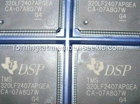
The TMS320LF2407APGEAG4 is a digital signal processor (DSP) controller. The TMS320LF2407APGEAG4 offers the enhanced TMS320 DSP architectural design of the C2xx core CPU for low-cost, low-power, and high-performance processing capabilities. Several advanced peripherals, optimized for digital motor and motion control applications, have been integrated to provide a true single-chip DSP controller. While code-compatible with the existing C24xDSP controller devices, the TMS320LF2407APGEAG4 offers increased processing performance (40 MIPS) and a higher level of peripheral integration. See the TMS320LF2407APGEAG4 Device Summary section for device-specific features. The TMS320LF2407APGEAG4 generation offers an array of memory sizes and different peripherals tailored to meet the specific price/performance points required by various applications. Flash devices of up to 32K words offer a cost-effective reprogrammable solution for volume production. The TMS320LF2407APGEAG4 offers a password-based code security feature which is useful in preventing unauthorized duplication of proprietary code stored in on-chip Flash/ROM. Note that Flash-based devices contain a 256-word boot ROM to facilitate in-circuit programming.
Parametrics
TMS320LF2407APGEAG4 absolute maximum ratings: (1)Supply voltage range, VDD, PLLVCCA, VDDO, and VCCA: - 0.3 V to 4.6 V, VCCP range: - 0.3 V to 5.5 V; (2)Input voltage range, VIN: - 0.3 V to 4.6 V; (3)Output voltage range, VO LF240xA: - 0.3 V to 4.6 V; (4)Output voltage range,VO LC240xA: - 0.3 V to 4.6 V; (5)Input clamp current, IIK (VIN < 0 or VIN > VCC): ± 20 mA; (6)Output clamp current, IOK (VO < 0 or VO > VCC): ± 20 mA; (7)Operating free-air temperature ranges, TA: A version: - 40℃ to 85℃, S version: - 40℃ to 125℃; (8)Junction temperature range, TJ: - 40℃ to 150℃; (9)Storage temperature range, Tstg: - 65℃ to 150℃.
Features
TMS320LF2407APGEAG4 features: (1)Controller Area Network (CAN)2.0B Module (LF2407A, 2406A, 2403A); (2)Serial Communications Interface (SCI); (3)16-Bit Serial Peripheral Interface (SPI)(LF2407A, 2406A, LC2404A, 2403A); (4)Phase-Locked-Loop (PLL)-Based Clock Generation; (5)Up to 40 Individually Programmable, Multiplexed General-Purpose Input/Output (GPIO)Pins; (6)Up to Five External Interrupts (Power Drive Protection, Reset, Two Maskable Interrupts); (7)Power Management: Three Power-Down Modes, Ability to Power Down Each Peripheral Independently; (8)Real-Time JTAG-Compliant Scan-Based Emulation, IEEE Standard 1149.1† (JTAG); (9)Programmable Deadband (Deadtime)Prevents Shoot-Through Faults; (10)Three Capture Units for Time-Stamping of External Events; (11)Input Qualifier for Select Pins; (12)On-Chip Position Encoder Interface Circuitry; (13)Synchronized A-to-D Conversion; (14)Designed for AC Induction, BLDC, Switched Reluctance, and Stepper Motor Control; (15)Applicable for Multiple Motor and/or Converter Control.
Diagrams

 |
 TMS3112 |
Other |
|
Data Sheet |
Negotiable |
|
||||
|
TMS3121 |
Other |
|
Data Sheet |
Negotiable |
|
||||
|
TMS320 |
Other |
|
Data Sheet |
Negotiable |
|
||||
|
TMS32010 |
Other |
|
Data Sheet |
Negotiable |
|
||||
|
TMS320AV7110 |
Other |
|
Data Sheet |
Negotiable |
|
||||
 |
TMS320BC51PQ100 |
Texas Instruments |
Digital Signal Processors & Controllers (DSP, DSC) TMS320C51PQ - 132QFP - 100MHZ/BOOT CODE |
Data Sheet |
Negotiable |
|
||||